Research and Development of Core Technologies for Next-Generation Semiconductor Microfabrication
Kentaro Tomita, and Katsumi Midorikawa
Key and Advanced Technology R&D through Cross Community (Collaboration Program) 2025.4.1~2027.3.31
A new project is underway to develop innovative semiconductor microfabrication technology “Made in Japan”
Semiconductors are often referred to in Japan as the “rice of industry,” a fundamental technology that supports modern society. Research and development into semiconductors is progressing on a global scale. Since 2024, Japan’s semiconductor industry has been undergoing a major revitalization, beginning with the opening of TSMC’s Kumamoto plant and the growth of semiconductor-related companies across Kyushu. In April 2025, Rapidus’s Institute for Materials Research and Development (IIM) in Chitose City, Hokkaido, launched a pilot line for next-generation 2-nanometer chips.
To ensure Japan remains competitive in the long run through research and development, the Cabinet Office initiated the Economic Security Key Technology Development Program (known as the K Program). A five-year project, “Next-generation semiconductor microfabrication process technology”, started in fiscal 2025 is one of its key initiatives.
Extreme ultraviolet (EUV) lithography is the most advanced exposure technology for semiconductor miniaturization and a key driver of innovation across multiple industries. Despite its potential, commercialization faces formidable barriers: EUV lithography systems require immense electrical power and carry price tags in the hundreds of billions of yen. The technology has already been adopted by Rapidus in Japan, yet so far only a single company in the world, the Netherlands-based multinational ASML, has succeeded in fully commercializing EUV lithography systems.
Semiconductor microfabrication project brought together Japanese institutions and experts with cutting-edge capabilities in EUV lithography, led by National Research and Development Agency RIKEN (Wako, Saitama Prefecture) to develop and disseminate foundational technologies capable of overcoming the major obstacles that EUV lithography still faces.
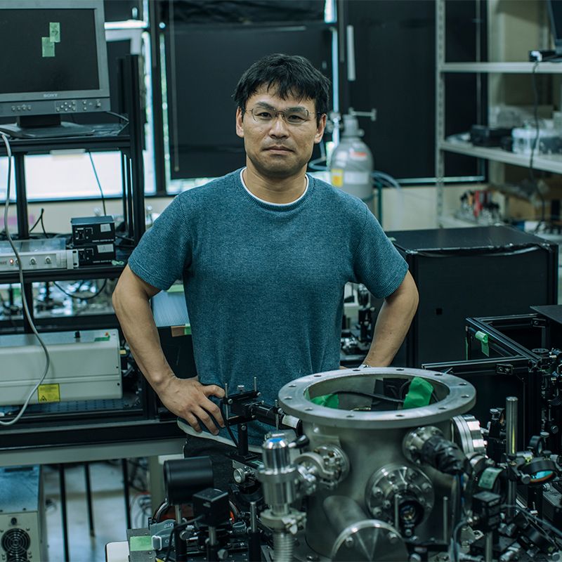
Associate Professor Kentaro Tomita is one of the project members and is expected to play a key role in advancing the understanding and control of plasmas for EUV light sources through precision measurements. Because of the properties of the multilayer mirrors used in lithography, the usable wavelength for EUV light is limited to around 13.5 nm. To generate this light, plasma is produced by heating tin (Sn) to approximately 300,000 degrees Celsius.
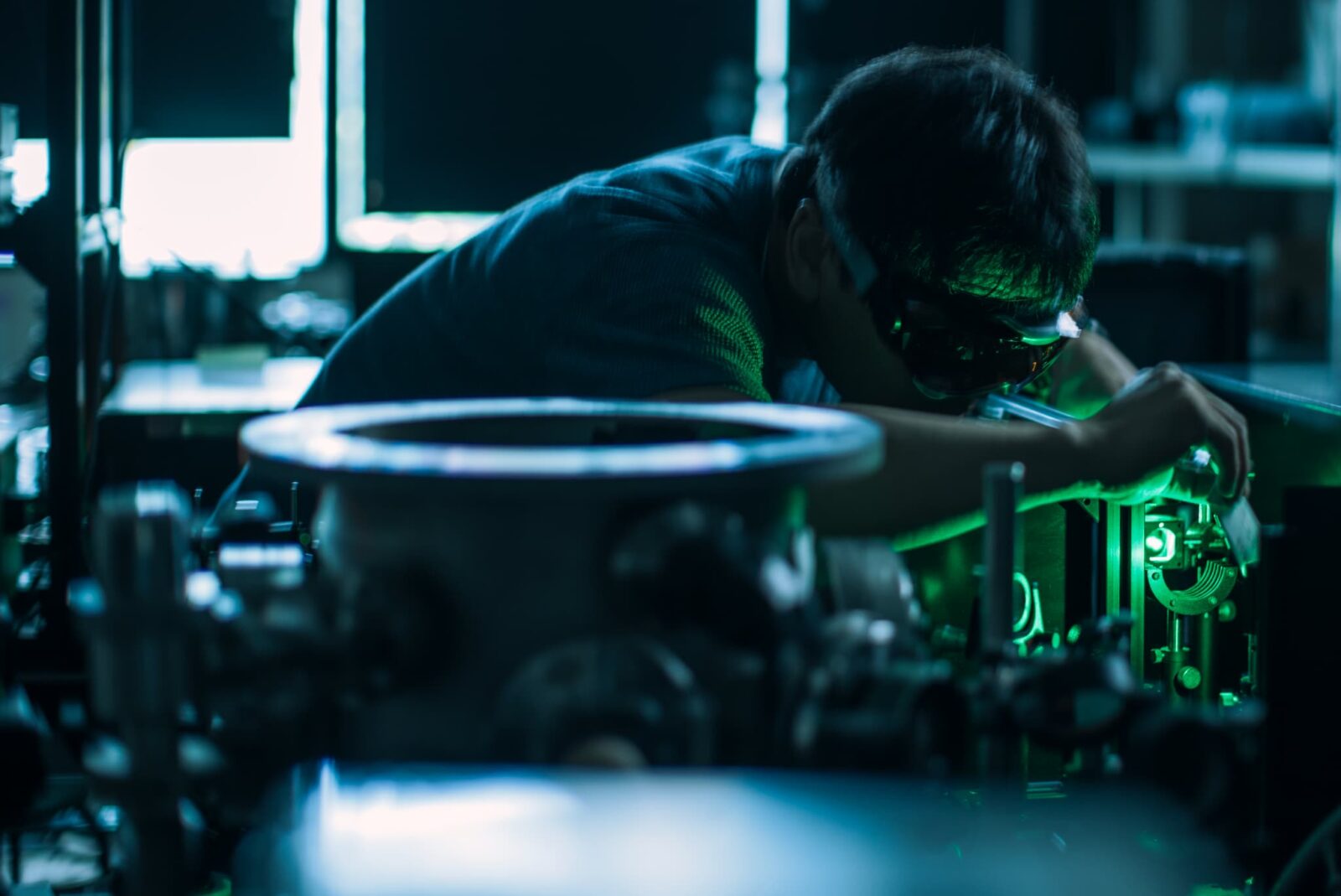
Controlling plasma temperature and density, optimizing the metal ion (valence) state, and preventing excessive EUV light absorption by the plasma itself (self-absorption) are key to achieving high-efficiency EUV light output. However, plasmas are notoriously difficult to control: they are short-lived (less than 100 nanoseconds), extremely small (about 0.5 mm in diameter), unstable, and non-uniform, while also exhibiting complex flows at speeds of tens of thousands of meters per second. Measuring their internal temperature and density has long been considered impossible.
Dr. Tomita has developed a unique laser-scattering technology capable of measuring plasma electron temperature, density, and flow fields in EUV light sources. His work is opening new frontiers in the optimization of EUV light sources.
Pursuing innovation through cross-disciplinary collaboration
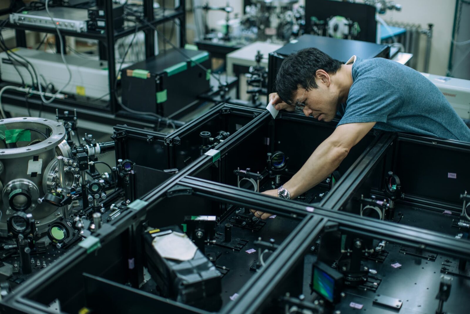
The advancement of EUV lithography brings together many underlying technologies. For example, the carbon dioxide lasers currently used for plasma generation in EUV lithography operate at a wavelength of 10.6 μm and suffer from extremely low plug-in efficiency (the conversion of electrical power into laser light). Developing new lasers with higher efficiency is just as important for the project as improving the efficiency of converting laser light into EUV light. Yet these challenges are typically tackled in separate research fields, and the conditions considered optimal in one are not always compatible with the other. This project therefore places strong emphasis on collaboration among specialists from diverse disciplines, united by a shared technological goal.
The project also includes other cross-disciplinary efforts, such as research on EUV-reflective mirrors and downstream microfabrication processes. As Professor Tomita notes, “By bringing together Japan’s leading experts across multiple fields, we have the chance to generate and share with the world truly innovative technologies.”

From fundamental science to industrial applications through measurement technologies
The K Program’s “Next-generation semiconductor microfabrication process technology” project is being carried out under an all-Japan semiconductor framework led by RIKEN. “This is my first time participating in a project of this scale, both in terms of personnel and budget. I am very excited about the opportunity to collaborate with researchers from different fields,” says Professor Tomita. He also emphasizes, “Measurement technologies play a crucial role in converting fundamental scientific knowledge of plasmas into applications that benefit industry and society.”
To promote the development of semiconductor talent, Hokkaido University established the Semiconductor Frontier Education and Research Center in April 2025. Through Professor Tomita’s involvement, the university’s younger researchers will gain invaluable opportunities to learn from the project. With the expectation that “fast-paced research on a five-year horizon is exactly where young talent should shine,” the project is now taking its first steps toward shaping a new era.
*This work is supported by JST K Program Grant Number JPMJKP24M1, Japan.
Faculty of Engineering, Division of
Applied Quantum Science and Engineering
Associate Professor Kentaro Tomita